

First commercial ASML EUV chip in production
Electronics concern Samsung is starting series production of a chip made using the extreme ultraviolet machine of ASML. This signifies a definitive breakthrough for the company, located in Veldhoven in the Netherlands, concerning a technological project they have been working on for nearly twenty years.
Samsung announced production of its new chip earlier this week during the Tech Day in California's San Jose and in a press release. This is the first time that chips for commercial use are being produced using the extreme ultraviolet machine (EUV) developed by ASML. Until now, these machines were primarily used for testing.
Race for increasingly better-performing chips
For Samsung, this relates to the so-called 7LPP chip, where 7 stands for 7 nm (1 nm = 10-9 m), the characteristic dimension at which the transistors on the chip are made. Compared with the 10-version of the chip, the new one is 40% smaller, performs 20% better and requires 50% less energy, says Samsung. This is all part and parcel of the race to make chips that perform ever more efficiently.
Wavelength of light forms a barrier
Chip manufacturers are now running up against the limit of conventional lithography technology. That method uses visible light at a certain wavelength (193 nm), and that creates a barrier to how small production can go, even though manufacturers have come a very long way with various tricks. Extreme ultraviolet light has a much shorter wavelength (13.5 nm), making it possible to manufacture even smaller components for the chip.
‘With the introduction of its EUV process node, Samsung has led a quiet revolution in the semiconductor industry,’ said Charlie Bea, Executive Vice President at Samsung Electronics, in the press release.
Extreme ultraviolet difficult to handle
ASML, world leader in the production of the machines used to make chips, had to jump many technical hurdles to make the EUV machine. For instance, EUV light is absorbed by glass, which means you can't use lenses to project the image of the chip – the mask – sharply on the photosensitive layer on the wafer from which the chip is made. Instead, ASML had to use mirrors, which also required special coating layers to produce enough EUV light.
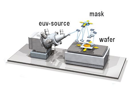
The biggest challenge was the EUV source, as there was no source that generated sufficient EUV light. ASML researched various possibilities, in the end opting for a Cymer system that fires a laser at droplets of tin. This prevents the vacuum chamber through which the EUV is projected from becoming contaminated with tin vapour.
Test machines
The first EUV test machines were delivered four years ago. Since then, the biggest challenge for the company has been ensuring that the machines achieve an adequate production speed. Success or failure is partly down to the exposure time required by the wafer in each production step. The more intense the EUV source, the shorter the exposure time and the faster the production.
The machine is being developed in close cooperation with chip manufacturers like Intel, Samsung and TSMC. The sector has jointly agreed a roadmap to facilitate EUV production.
If you found this article interesting, subscribe for free to our weekly newsletter!


Reacties